We use cookies to improve your online experience. By continuing browsing this website, we assume you agree our use of cookies.
Industry News

High-NA EUV lithography leads to halving the maximum area of a single chip, imec, Intel to find a way out

Views : 47
Update time : 2024-03-05 17:17:20
         With the rapid development of technology, the semiconductor industry is ushering in a brand new revolution. High NA lithography technology, as a representative of the next generation lithography technology, is expected to be officially put into use in the coming years. However, this disruptive technology also brings a serious challenge: the maximum area of a single chip is facing the dilemma of halving. Faced with this challenge, global semiconductor giant Intel and renowned Belgian semiconductor research institution IMEC have taken action one after another, striving to find a solution.
        The emergence of High-NA lithography technology was originally aimed at achieving more precise lithography effects and improving the accuracy and efficiency of chip manufacturing. However, due to the use of deformable lenses in this technology, the reduction magnification in the X and Y directions is different, resulting in a halving of the field of view size. This means that in the High-NA lithography era, large area chips like GA100 on Nvidia A100 computing cards will be difficult to manufacture using a single chip solution. This undoubtedly brings enormous challenges to the semiconductor industry.
        On February 29th, it was reported that Intel and Belgian semiconductor research institution IMEC have recently provided solutions to this issue.
        In current lithography, the maximum area (field of view) of a single chip is 26 * 33=858mm2. It is understood that in order to achieve more precise lithography results, the High-NA lithography machine uses deformable lenses, resulting in different reduction rates in the X and Y directions, and the field of view size is halved to 26 * 16.5=429mm2. Taking NVIDIA chips as an example, the GA100 core area on its A100 computing card is as high as 826 mm ²Approaching the current upper limit of area; In the High-NA lithography era, the maximum area of the chip could not reach 445mm of the TU106 core used for graphics cards such as RTX 2070 ²A reduced field of view means that large chips are difficult to manufacture using a single chip solution. Intel and IMEC have each proposed solutions for this.
        Intel CEO Pat Gelsinger stated in an interview with technology blog More Than Moore that he is exploring the possibility of using larger masks with partners such as ASML. The field of view size is related to the size of the mask. Currently, the industry generally uses 6-inch * 6-inch masks, and by doubling the mask size (6 inches * 12 inches), the field of view size of High-NA lithography can be restored to the current level.
        According to Bits&Chips, the industry had previously rejected the option of doubling the mask size in High-NA EUV lithography because it was believed that using the existing EUV mask size would be more cost-effective at the time. However, now Intel, as the most enthusiastic supporter of High-NA EUV, hopes to reopen the discussion on this matter. On the other hand, IMEC stated that it will showcase the prototype of field of view stitching technology at the 2024 SPIE Advanced Lithography and Patterning Conference this week. This scheme completes two half field scans during exposure, and the two parts are spliced to form a full field pattern. IMEC stated that it will share the latest insights on implementing field of view stitching technology on existing 0.33NA EUV lithography machines and believes that this solution can reduce the need for design changes in response to field of view reduction in the High-NA era.
        Of course, both Intel's larger mask scheme and IMEC's field of view stitching technology require further research and verification before they can be practically applied. In this process, the semiconductor industry still needs to face many challenges and difficulties. However, we believe that with the joint efforts of global researchers, these challenges will eventually be solved.
Related News
Read More >>
Qingming Festival holiday notice Qingming Festival holiday notice
Apr .02.2024
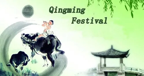
On April 4th, it is the traditional Chinese festival Qingming Festival. According to traditional customs, we will return to our hometown to worship, ancestor worship, and tomb sweeping. We will enjoy a three-day holiday and return to our hometown to worsh
Microchip Technology Announces Qi® v2.0 Compliant, dsPIC33-Based Reference Designs Microchip Technology Announces Qi® v2.0 Compliant, dsPIC33-Based Reference Designs
Mar .30.2024
Microchip has officially released the ISO 26262 functional safety package for dsPIC33C digital signal controllers (DSC), PIC18, and AVR microcontrollers (MCU), accelerating the development of safety critical designs for ASIL B and ASIL C safety levels and
Easter Notice Easter Notice
Mar .29.2024
During the Easter holiday, SIC Electronics’ companies in the United States, Hong Kong, and the United Kingdom are on holiday, but employees of the Chinese company work normally.
Infineon launches low-cost, low-power, long-distance Bluetooth module CYW20822-P4TAI040 Infineon launches low-cost, low-power, long-distance Bluetooth module CYW20822-P4TAI040
Mar .28.2024
Infineon Technology Co., Ltd. recently announced the launch of the latest Bluetooth module CYW20822-P4TAI040, which has achieved new breakthroughs in low power consumption and coverage, promoting the further development of wireless connection technology i